Using gEDA
ArticleCategory: [Choose a category, translators: do not translate
this, see list below for available categories]
Applications
AuthorImage:[Here we need a little image from you]
![[Photo of the Author]](../../common/images2/article355/iznoT2.png)
TranslationInfo:[Author + translation history. mailto: or http://homepage]
original in en Iznogood
AboutTheAuthor:[A small biography about the author]
Involved in GNU/Linux for a while, I'm now running a Debian
system. Despite electronic studies, I've mostly done a translation work for the
GNU/Linux community.
Abstract:[Here you write a little summary]
How to develop some Printed Board Circuits with free tools from the
gEDA community.
ArticleIllustration:[One image that will end up at the top of the
article]
![[Illustration]](../../common/images2/article355/logo.png)
ArticleBody:[The main part of the article]
Introduction
Why another article to talk about EDA, Electronic Design Automation?
Because there is more than one way to do it and this one is free. One of
its best particularity is the fact that we have a set of tools, some
graphical ones but mostly command line based. With this article, I will just
show how to make a PCB (Printed Circuit Board) from the beginning.
What is gEDA?
Most important, gEDA is a set of free (in the GPL way) electronic tools.
It is therefore always in development state.
I put here
the gEDA diagram. Click on it to enlarge.
![[Illustration]](../../common/images2/article355/gEDA1.png)
In the center, we have gschem, the graphical schematic and symbol
editor.
It can be called by geda, the manager, on top of gschem. With it, you
can not only launch gschem but a spice simulator, a pcb designer, a
gerber and a waveform viewer.
On the top left, with tragesym, you can create symbols and gsymcheck
will check them.
Most interesting for us, down gschem, we have
two ways of doing net-lists. It is a gEDA particularity: every exchange
file is in plain text, only the extension indicate the goal:
- .sym for symbols files
- .sch for schematic files
- .net for net-list files
- .pcb for pcb files and so on...
You have gnetlist, the "official" way to do net-listing for spice
simulation with tclspice, ngspice, gnucap, Verilog synthesis with
Icarus or PCB creation. gsch2pcb is a net-lister dedicated for pcb. It
does the translation from .sch file components to pcb file, back
and forth. And to finish, we check the pcb file with gerbv.
In this article I will only talk about gschem, gsch2pcb and PCB. We
will begin with gschem.
Placing components with gschem
I won't talk a lot about installation: apt-get install geda-gschem
geda-symbols geda-utils pcb for GNU/Debian.
On others systems,
download the required files on http://geda.seul.org/source.html,
http://pcb.sourceforge.net/ for PCB and ./configure & make &
make install as usual.
Ok, let's open gschem. We have two ways to do it: we open it with the
command gschem alone or we put a filename like: gschem sample.sch. Now
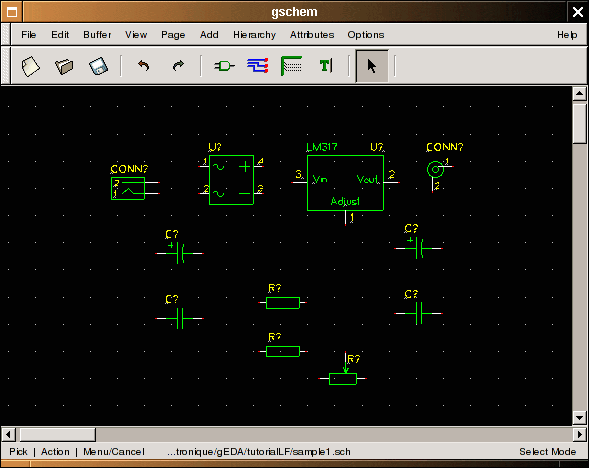
we can place components: one more time, we have two choices: with the mouse
and "Add Component" or from the keyboard with "i". We select BNC-1.sym,
pwrjack-1.sym in connector, 2 resistor-2.sym, 1
resistor-variable-2.sym, 2 capacitor-1.sym, 2 capacitor-2.sym,
bridge-1.sym in analog, lm317-1.sym in linear.
We will have this picture as result:
Don't worry, you can download all files
from
my homepage (updated) or from
this server.
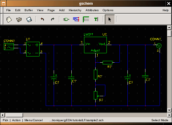
Now we can wire the components. To do it, we need to move them
and make rotations. Since we are lazy people, we will use keyboard
shortcuts: click on component then "er" for rotation, "ei" for
mirroring, "m" for moving, and "n" for wiring the components. We can
select only the part name to move or rotate it.
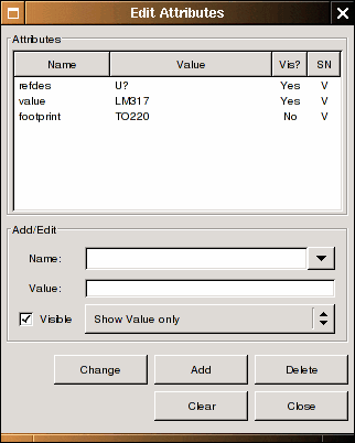
Once done, we can edit each component attribute with "ee". We can begin
with the most important component : LM317. When we open the attribute
box, we can see this:
We write LM317 into value name and TO220L for footprint (make it
invisible). For resistors, the value is indicated above on the schema
and the footprint is R025. And so on for capacitors,
potentiometers (you can see the sample.sch file added to the
article)...
Once we have finished, we can save it with a "fs" if the file have a
name and "fa" otherwise.
Translation with gsch2pcb
First, we need to give a number to the parts with the command:
refdes_renum sample.sch
If we reopen the file, we will see all ? from R?, C? U? changed to a
number. This mean we can make a net-list. First we must
install some footprint library and make a project file. We need to do
it because there is a lack of documentation for pcb footprint use
with gschem or I haven't found it. A good footprint set can be found
here :
http://
web.wt.net/%7Ebillw/gsch2pcb/gsch2pcb-libs.tar.gz. (local copy)
Download and install it with:
mv gsch2pcb-libs.tar.gz ~/toTheLocationYouWant/
tar xvzf gsch2pcb-libs.tar.gz
Then you
can make a project file with:
schematics sample.sch
elements-dir ~/XXX/pcb-elements
output-name sample
I have named it sampleLFprojet but you can use the name you want.
The schematics is for our gschem file. Elements-dir gives to pcb the
footprint directory to use (replace XXX with your directory location
for
pcb-elements). And the output-name is to continue with the sample name
for pcb. We save it in the same sample.sch directory.
The next step is to run:
gsch2pcb tutorialLFprojet
The output are files named sample.board and sample.net. The first one
lists all
component parts to be used with PCB and the second one is the net
listing.
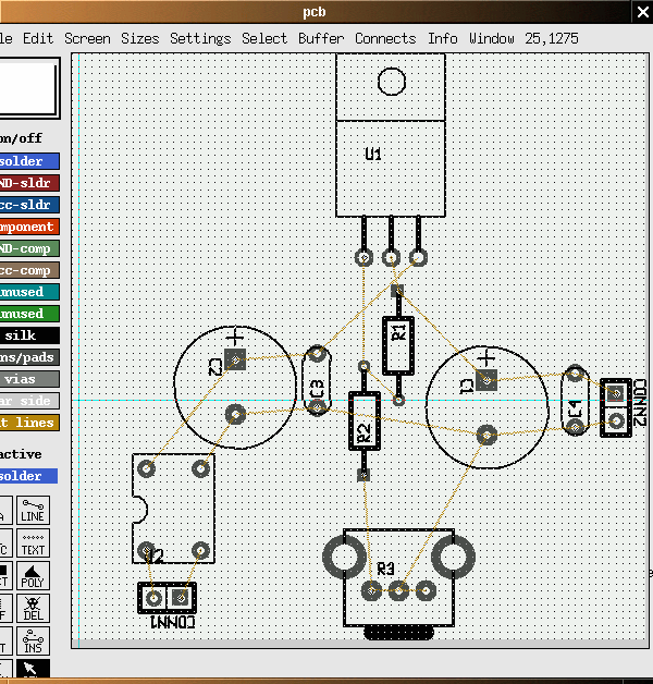
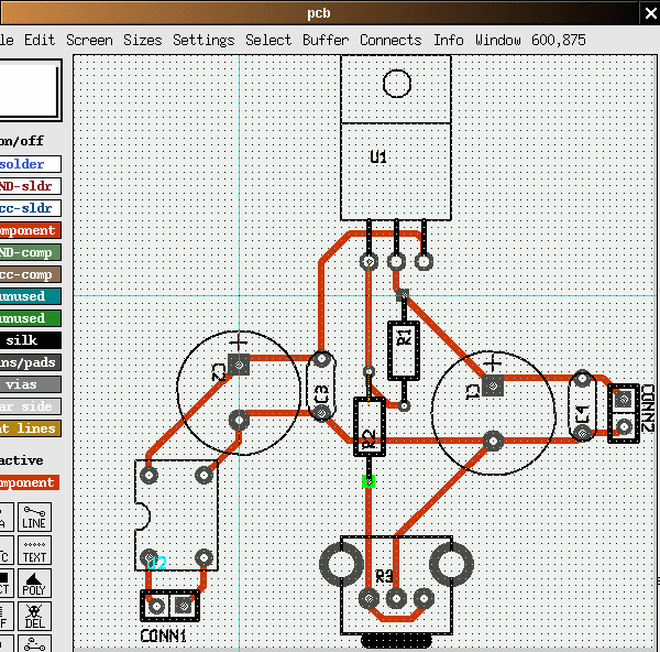
Making a circuit with PCB
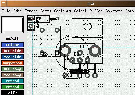
We can start now with PCB. Open :
pcb sample.pcb
You will have this picture :
All components are packed to the left up side. We need to place the
components on the board. Then we call the wires (nets) with the
sample.net file with File --> load net-list file and optimize Connect
--> rast-nets. It's quite magic.
Now we place nets as desired with Line and solder mask selection.
It's finished: you just have to save and make a File --> print layout
to have your pcb printed.
Conclusion
The goal of this article was just to have a straight and rough
introduction to of some of the gEDA tools available and to show an easy,
short way to make a PCB. But gEDA is so much more that it will take
you a long time to play around with it: you will need to make a lot of
optimizations to make an output usable for professional pcb makers.
Related articles
This article is mainly influenced and based on the Bill Wilson
bill--at--gkrellm.net documentation gsch2pcb.html.
And you can find more information at www.geda.seul.org.
PCB can be found at pcb.sourceforge.net.
If you understadn french then you can find more on
http://www.iznogood-factory.org
and for english speaking people, there is some stuff
here.
![[Illustration]](../../common/images2/article355/gEDA.png)